SIP RESISTOR NETWORK----------------------------------------------------------

RA•RB SERIES

Thick film resistor network have Metal Glaze element on the
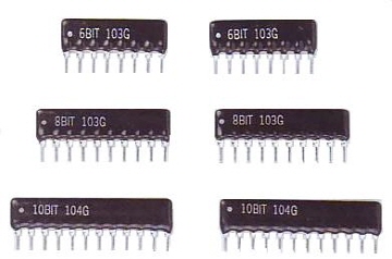
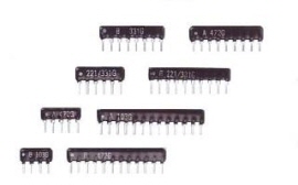
ceramic substrates with strong clip construction terminal,
and are coat with special epoxy resin. They are the most
suitable to meet the density of circuit assembling.


Application
Control Circuits of V.T.R Computer, Facsimile, Car &
Air-Conditioner
Color T.V & Other Electronic equipments for Consumer
use.


FEATURES
Miniature,High Density Packaging
Combinations of Different Ohmic value are available.
High Reliability with RUO2 Paste.
TYPE L
(MAX)
H
(MAX)
T
(MAX)
C
+0.3
-0.2
d
±0.05

f
±0.2
RA RB
4 pin 10.2 5.08 7.5 2.5 2.8 0.5

2.54

5 pin 12.7
6 pin 15.3
7 pin 17.8
8 pin 20.4
9 pin 22.9
10 pin 25.4
11 pin 28.0
12 pin 30.5
13 pin 33.1
14 pin 35.6

RATING
Operating Temp. Range -55¡É ~ +125¡É Wattage/Element RA RB
T.C.R ±100PPM 50Ω ~ 2.2MΩ B Style Others All Style
±250PPM < 50Ω or ≥ 2.2MΩ 0.2W 0.125W 0.25W
Rating Ambient Temp. +70¡É Max. Working Voltage 100V 200V
Resistance Ranfe
(E-12 Series)
R Style Others Resistance Tolerance F=±1%,G=±2%,J=±5%
100Ω ~10K 10Ω~4.7MΩ

CIRCUIT CONSTRUCTION
A B C D
E P T R

CHARACTERISTIC
ITEM TEST METHODS SPECIFICATIONS
Resistance Temperature Characteristic -55¡É ~ +125¡É ±100ppm/¡É for 50Ω~2.2M
±250ppm/¡É for < 50Ω ≥ 2.2M
Temperature Cycling -55¡É ~ +125¡É, for 5 Cycle ¡âR ≤ ±(0.5% + 0.05Ω)
Short-Time Overloard Rated Voltage X 2.5 for 5sec. ¡âR ≤ ±(0.5% + 0.05Ω)
Resistance to Soldering Heat 350¡É for 3sec ¡âR ≤ ±(0.5% + 0.05Ω)
Insulation Resistance 100V for 1minute ¡â 10,000MΩ Min.
Terminal Strength Tensile : 1Kg, 30 sec
Bending : 500g, 2Times
¡âR ≤ ±(0.25% + 0.05Ω)
Thermal Shock Load V, Room Temp.30 minute
Unload, -55¡É, 15 minute
Over 2hrs in Room Temp. before measuring
¡âR ≤ ±(0.5% + 0.05Ω)
Solderbility 230¡É ± 5¡É, 3sec Covering 95%
Moisture Load Life 40¡É, 90~95% RH rated Voltage for 1000 hours ¡âR ≤ ±(2% + 0.05Ω)
Load Life 70¡É at Rated Voltage for 1000 hours ¡âR ≤ ±(2% + 0.05Ω)

STANDARD RESISTANCE (OHM) E-12 SERIES
10 12 15 18 22 27 33 39 47 56 68 82
100 120 150 180 220 270 330 390 470 560 680 820
1K 1.2K 1.5K 1.8K 2.2K 2.7K 3.3K 3.9K 4.7K 5.6K 6.8K 8.2K
10K 12K 15K 18K 22K 27K 33K 39K 47K 56K 68K 82K
100K 120K 150K 180K 220K 270K 330K 390K 470K 560K 680K 820K
1M 1.2M 1.5M 1.8M 2.2M              


DUAL TERMINATORS (R1/R2) (OHM)

DUAL TERMINATORS (R1/R2) (OHM) DERATING CURVE
160/240 330/390
180/390 330/470
220/270 1.5K/3.3K
220/330 3.0K/6.2K


HOW TO ORDER


THICK FILM R/2R LADDER NETWORKS---------------------------------------------------


BITS Number
of pins
Lmax.
(mm)
4 6 15.3
5 7 17.8
6 8 20.4
7 9 22.9
8 10 25.4
9 11 28.0
10 12 30.5
  4BITS 5BITS 6BITS 7BITS 8BITS 9BITS 10BITS
Standard Resistance value 5KOhm - 10KOhm - 25KOhm - 50KOhm - 100KOhm
Bit errors

±1/2LSB

FSA (Max.) 3.12% 1.56% 0.78% 0.39% 0.2% 0.2% 0.2%
Output Impedance
Characteristic
±2%
Rated Voltage 30mW/element
Working Voltage DC 20V Max.
Operating Temp.
Range
-55¡É ~ +125¡É


CIRCUITS DIAGRAM  
Part No. Circuits Marking
RAL 4BIT 503G •4BIT 503G
RAL 5BIT 503G •5BIT 503G
RAL 6BIT 503G •6BIT 503G
RAL 7BIT 503G •7BIT 503G
RAL 8BIT 503G •8BIT 503G
RAL 9BIT 503G •9BIT 503G
RAL 10BIT 503G •10BIT 503G